Personal project·Jun – Aug 2026Complete
Heart Rate Monitor PCB
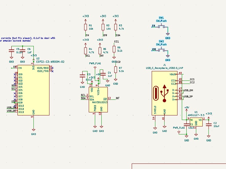
A 2-layer mixed-signal board in KiCad pairing a MAX30102 optical sensor with an ESP32-C3, taken from schematic through assembled bring-up.
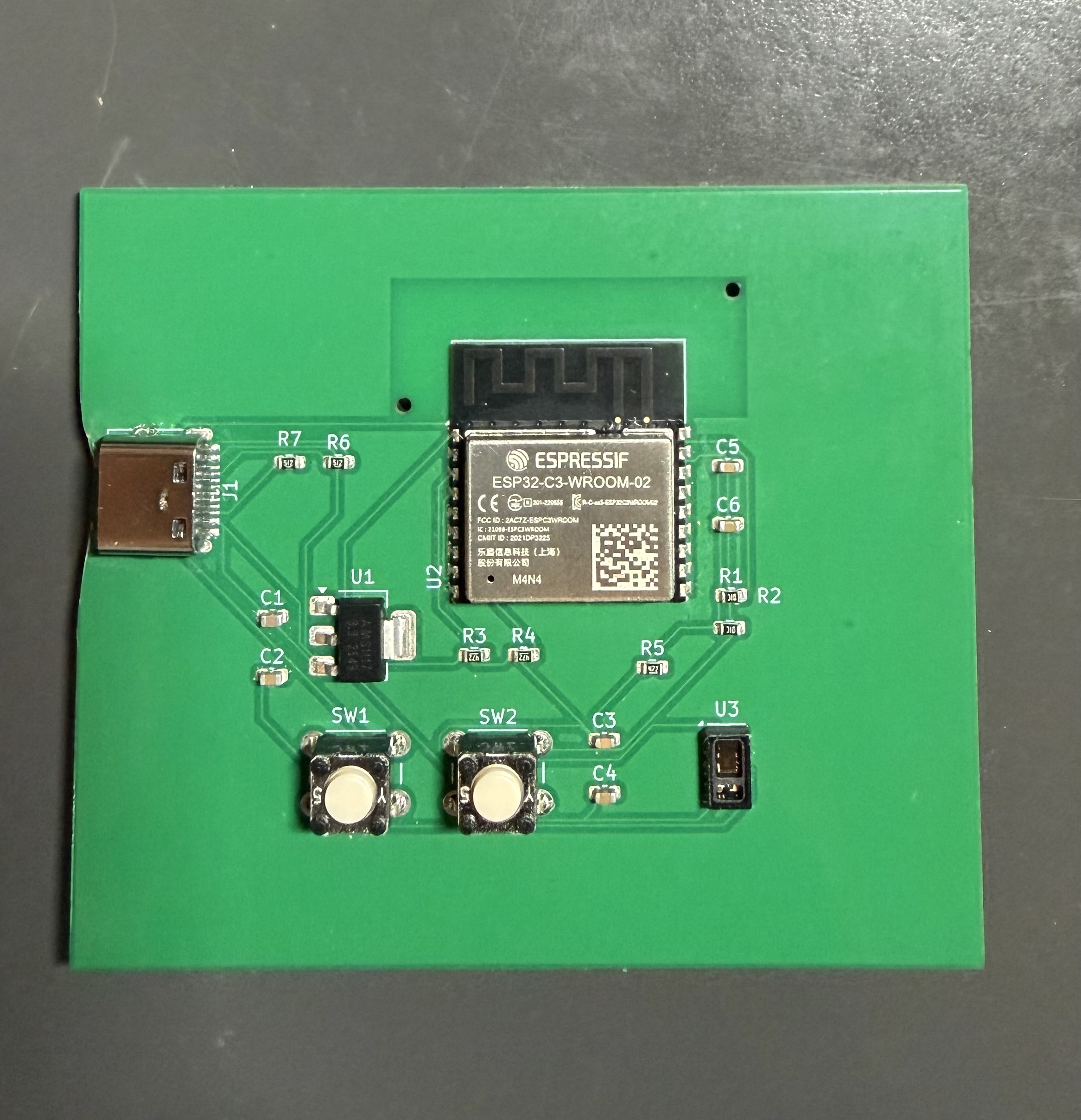
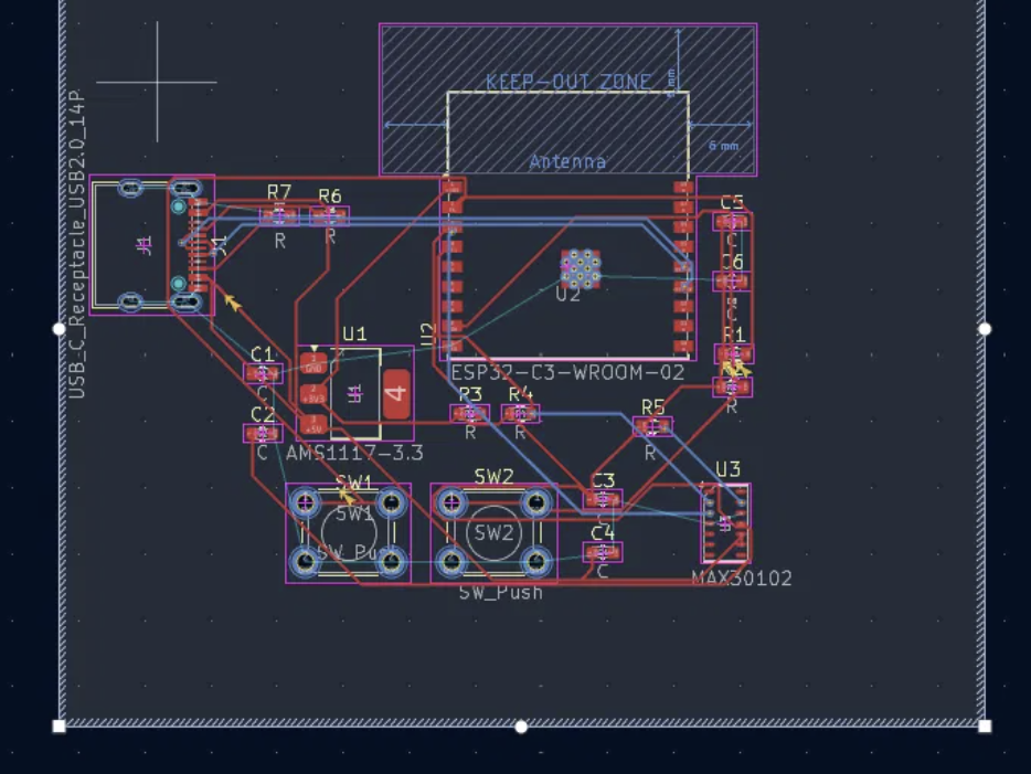
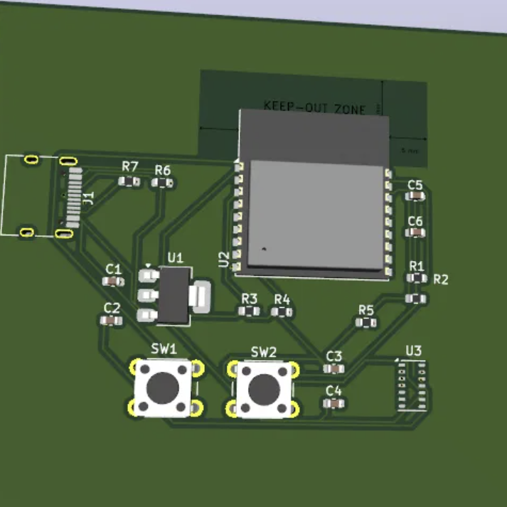
A mixed-signal board designed from scratch in KiCad: schematic capture, footprint assignment, layout and routing, DRC resolution, and Gerber/BOM/CPL generation for assembly. The MAX30102 handles PPG sensing, an ESP32-C3-WROOM-02 processes it over I2C, and an AMS1117-3.3 LDO delivers a stable 3.3 V rail from USB-C.
Highlights
- Laid out a 2-layer, 70×60 mm board with ground pours on both layers and local 100 nF / 10 µF decoupling
- Prepared Gerber, BOM and CPL files for a JLCPCB assembled order, fixing a BOM export error and the CPL format
- Brought up the board by reworking a USB-C opening blocked by excess board material, then confirmed a pulse reading in firmware